About Us
ProTrusTech (PTT) stands for Professional, Trust, Technology—the Company’s core values. Providingprofessional service, building reliability with customer, devoteing to Ramansystem manufacture and development. Our Raman system have sold in countriessuch as Taiwan, Asia, Europe, and Japan. We never stop developing steps so as toupgrade convenience of hardware operation and meet marketing request ofsoftware function. Therefore PTT also could provide customize product and OEM& ODM Raman service to meet marketing request.

 
PTT not only haveRaman spectrometer building from Taiwan brand, also provides precisioninstrument measurement equipment required for materials science, includingnanogenerators, Thin Film Coating,
stackermicrofluidic nanoparticle synthesizers, lasers, micro spectroscopy, atomicforce microscopes, surface photovoltage spectroscopy, etc., which can realizematerial analysis, Semiconductors, solar energy industry, biology, chemistry,medicine, gemstones, customs trade, agriculture, animal husbandry, electronicsindustry and other fields.
ProTrusTech substantially believes that success comes from both customer satisfaction and our innovation. Building on our expertise in customization and patented technology, we developed a range of high-quality and reliable products: MRI, MRID, GMD, GMDX and RAMaker.


Whether you have training in the relevant field or not, we can provide you with the right product including research-grade or simple Raman for you to choose.


Manufacturers for foundry and OEM  
We can offer OEM/ODM services to serve a wider range of companies. Due to application of Raman spectroscopy has become wider. Therefore, based on many years of experience, we have designed an one-piece-formed with more stable optical module, which can mass produce both macro and micro Raman spectrometers, so that Raman spectroscopy can be used in various fields more universal. In addition to its own brands, PTT also seeks for cooperative manufacturers for foundry and OEM.
US Patent : US10,247,674B2
US Patent : US11,340,114B2


History
2023, Invention Platinum Medal Award 
2023, Futue tech Award
2023, Innovative Improvement Award
May 2019, US Patent US10,247,674B2
July 2019, collaborate with NCHU about SERS
April 2018, Get order from India
February 2018, Japan distributor
October 2017, US Patent pending
August 2017, Get Taiwan patent I593953
January 2017, Get Taiwan patent I570402
December 2016, Get order from Sweden and China
October 2016, Publish in Faraday Discussions international journal of AIEE application of micro Raman spectroscopy
January 2016, US, China and Taiwan patent pending 
September 2015, SBIR
January 2015, Apply for US patent
November 2014, First contract of oversea distributor
June 2014, MRI Micro Raman spectrometer
April 2014, Get Taiwan patent M475582
February 2013, Micro Raman spectrometer
December 2011, PRRS surface enhanced kit
November 2011, 266 nm UV Micro Raman
August 2010, RAMaker micro Raman spectrometer
November 2008, Establish


We can provide
‧ Raman spectroscopy
‧ PhotoLuminescence
‧ PhotoReflectance
‧ Tip-Enhanced Raman Scattering
‧ Surface Enhanced Raman Scattering
‧ ElectroLuminescence



Hot Products
MRID
MRID
Video Reference
Polarized Micro Raman
Dual Lasers Auto switch Micro Raman Spectrometer
Polarized Micro Raman system --- ProTrusTech MRID
Raman Polarization Rotating Mapping (RPRM)---PTT Auto Raman Spectroscopy
Auto scan polarization micro raman spectroscopy
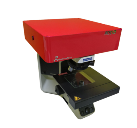
MRID (Micro Raman Identify Dual Lasers)


TheMRID (Micro RamanIdentify Dual Lasers) system is protected bypatents in Taiwan (I709732) and the United States (US 11,340,114 B2). Thispatented design is based on an optical setup with built-in direct light path,dual-laser sources and dual spectrometers. Software controls the switchingbetween different laser wavelength to achieve fully automatic microscopic Ramanlaser source selection, requiring no manual adjustments. Combined with thehighly stable optical system, which eliminates the need for an optical table,the overall design significantly reduces operational complexity, allowing evenusers without any background to operate the system easily.
TheMRID features a horizontally interleaved optical light path and can becustomized with a third or additional laser sources via fiber input accordingto customer requirements, making it convenient for users to switch lasers oradapt the system for other applications.


Dual- Laser Measurement  


Independentlydeveloped by Protrustech andprotected by a patent, the dual-laser system allows users to measure Ramansignals from different laser wavelengths with a single button click. As shownin the figure, a silicon wafer under a 785 nm laser get a peak at 520 cm-1 andshows thermal effects in the NIR range. Another Raman spectrum illustrates thetypical response of a silicon wafer under a 532 nm laser. This design can alsobe customized to:
•Use asingle laser source to simultaneously measure Raman and fluorescence orphotoluminescence signals. •Usedual laser sources for simultaneous measurement. •Measureseparately with dual laser sources while displaying both results on the screensimultaneously.


Two type of laser power controllinginterface


Two software-controlled methods areavailable for laser power adjustment. A continuous neutral density filters (O.D.2.0~0.04) with a built-in laser power calibration curve allows precise controlwith accuracy of better than 1%. Both default and user-defined laser powertransmittance (%) are supported. Additionally, laser output power can beadjusted via software in 1 mW steps.
By combining these two controlfunctions, the laser power can be finely tuned to a minimum output of 0.01 mW 1%.


ND control : User-input & frequentiy usedtransmission     
     

Laser control : User input,1mW/step


Angle Resolved Polarized Raman
TheRPRM (RamanPolarization Rotating Mapping) function is designed forhighly crystalline or 2D materials . When measuring polarization-dependentRaman differences, the software can automatically rotate the polarizer of thelaser and signal with different angles; the system also can automaticallydefine the zero of the laser and signal polarizer angle . This facilitatesresearchers in observing the lattice arrangement of the sample.


Automatic Switching  Raman Measurement (SCAN) / SampleObservation (VIEW)


Themicroscopic Raman system designed by Protrustech uses a 5-megapixel CCD paired with a 5WLED light source for sample imaging. During sample positioning, the laser poweris automatically reduced to below 0.1% to balance the brightness between thelaser and the white light. This allows clear observation of the sample surface,enabling precise laser positioning and accurate surface focusing.

Whenswitching between Raman measurement and sample observation, the software canperform automatic switching, eliminating the need for manual adjustments andpreventing sample displacement caused by vibration during manual switching. Thelaser spot position tolerance on the sample is within 1 μm.


    Non-reduced laser power              After auto reducing laser power


Ramanmapping system

- MaximumScanning Range: 75×50 mm or 100×100/ 200×200 mm - MinimumXY step size (Resolution): 0.05 µm
- Repeatability : <1 µm - MinimumZ step size (Resolution): 0.002 µm depend on microscopespecification - Themotorized stage can be controlled via mouse click(XY) and scroll wheel (Z) - Additionaldata analysis software - Observationimage and Raman Image center calibration function - Autofocusing function by Raman signal intensity or observation image


4-Point Probe / Temperature Control
Microscope Stage(Optional)
Vacuum temperature control :-196 ~ 350/600℃ Heating stage :up to 1500℃ Four-point probe measurements


EC-RAMAN     


CombiningElectrochemical and Raman spectroscopies can provide more detailed informationabout electrode reactions. We refer to this dual-function system as CombinedEC-Raman. The Combined EC-Raman enables in-situ measurements with real-timemonitoring and recording to track structural changes and identify adsorbedproducts or intermediates.
Wehave integrated the CHI electrochemical stage with our MRI micro-Ramanspectroscopy. Depending on the electrolyte used, users can configure differentlaser wavelengths for Raman measurements, or automatically switch between 532nm and 785 nm laser sources. After the experiment, Raman spectra from bothwavelengths can be obtained for comparison.
TheCombined EC-Raman system is designed to provide richer and more immediateinformation, making it a powerful tool for electrochemicalresearchers.(Patents: Taiwan I 750718, U.S. 11,340,114 B2)


STMTERS (Upgrade,Taiwan only)
TheMRI/MRID system can be combined with an STM (Scanning Tunneling Microscope) tocreate a localized resonance region at the tip, enhancing the Raman signal.This technique is known as TERS (Tip-Enhanced Raman Spectroscopy). Thislocalized resonance region is commonly referred to as the “hot spot.” Withinthis region, the nanometer-scale precision of the STM enables the detection ofRaman signal variations with spatial resolution down to several tens ofnanometers.
ReferenceSpecifications
• TheMRID optical system can be configured with two built-in lasers simultaneously.It employs compact and highly stable lasers from RGB Lasersystems (Germany). Depending on Raman orfluorescence applications, users can select laser wavelengths such as 375, 405,473, 532, 633, 785, 808, or 830 nm. • Thecommonly used 532 nm laser operates in TEM₀₀ mode, with an optimal output beamdiameter of 1.2 mm. When focused through a 100X objective lens, the laser spotsize on the sample can be reduced to less than 2 µm. Available objectivesinclude 10X, 40X, 50X, 100X, or others upon request. • TheRaman spectral range can be customized according to user requirements. Using ahigh-performance edge filter, measurements can start from 50 cm-1, depending on the laser wavelengthand sample. –For a standard 532 nm setup:
   ►Range: 79~3500 cm-1, Resolution: 1.8 cm-1
   ►Range:79~2100 cm-1, Resolution: 1.3 cm-1
   ► Example:The 85 cm-1 Raman signal of sulfur can beclearly detected.
–For 785 nm, the typical range is 150~3500 cm-1with 1.8 cm-1 resolution.
–Other ranges depend on the selectedlaser wavelength.
Each system is supplied withsilicon or sulfur reference samples for calibration.


Applications